Optimized 3 nanometer (nm) process, with a 23% improvement in performance and a 45% reduction in power consumption
Compared to 5 nanometers (nm), the chip area is reduced by 16% and

As one of the advanced semiconductor technology manufacturers, Samsung Electronics announced today that chips based on the 3-nanometer (nm) Gate All SurroundT (GAA) process node have begun preliminary production< Br/>
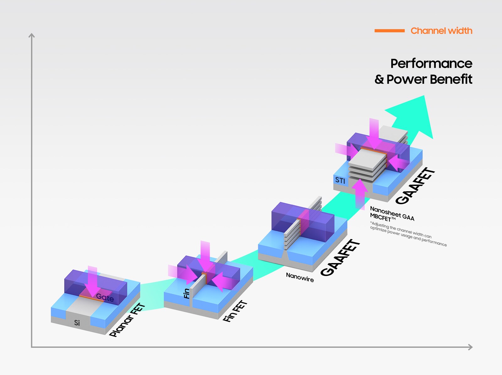
Samsung Electronics Achieves GAA for the First Time; Multi bridge channel field-effect transistor; The application of MBCFET™ Multi Bridge Channel FET breaks the performance limitations of FinFET technology by reducing the operating voltage level to improve energy consumption ratio, and also enhances chip performance by increasing driving current. Samsung first applied nanoscale transistors to semiconductor chips in high-performance and low-power computing, and plans to expand them to the field of mobile processors< Br/>
Dr. Siyoung Choi, President and Head of OEM Business at Samsung Electronics, stated:; Samsung Electronics has been continuously applying new generation process technologies to production and manufacturing. For example, Samsung's first High K Metal Gate (HKMG) process, FinFET, and EUV. Samsung hopes to adopt the 3nm process for the first time; Multi bridge channel field-effect transistor; MBCFET™ will continue to maintain its leading position in the semiconductor industry. Meanwhile, Samsung will continue to actively innovate in competitive technology development and establish processes that help accelerate technological maturity< Br/>

Optimization of technical design to maximize the benefits of PPA [1]
The 3-nanometer (nm) GAA technology uses wide channel nanosheets, which can provide higher performance and energy consumption compared to the GAA technology using narrow channel nanowires. In terms of 3-nanometer GAA technology, Samsung can adjust the channel width of nano transistors, optimize power consumption and performance, and thus meet the diverse needs of customers. In addition, the design flexibility of GAA is very advantageous for Design Technology Collaborative Optimization (DTCO) [2], which helps to achieve better PPA advantages. Compared with the 5 nanometer (nm) process, the first generation 3 nanometer (nm) process can reduce power consumption by 45%, improve performance by 23%, and reduce chip area by 16%; The second generation 3 nanometer (nm) process reduces power consumption by 50%, improves performance by 30%, and reduces chip area by 35%< Br/>
Compatible with SAFE™ Collaborate with partners to provide 3-nanometer design infrastructure and services
As process nodes become smaller and chip performance requirements increase, IC designers need to face the challenges of processing massive amounts of data and verifying complex products with more functionality and tighter scalability. To meet these needs, Samsung is committed to providing a more stable design environment to help reduce the time required for design, verification, and approval processes, while also improving product reliability. Since the third quarter of 2021, Samsung Electronics has been cooperating with Samsung's advanced Foundry model ecosystem SAFE™ The close collaboration of Samsung Advanced Foundry Ecosystem partners provides a mature/reliable design infrastructure that enables them to improve their products in a shorter period of time< Br/>
From SAFE™ Partners
&Bull; ANSYS, [John Lee, Vice President and General Manager, Electronics, Semiconductors, and Optics Business Unit, Ansys]" ANSYS and Samsung collaborate to continue providing support technology for state-of-the-art designs using 3nm GAA technology. At present, the signing accuracy of Ansys Multiphysics simulation simulation platform ensures our continuous partnership with Samsung Foundry model, which is at the forefront of the industry. Ansys is always committed to providing the best design experience for our common and important customers& Rdquo< Br/>
&Bull; Tom Beckley, Senior Vice President and General Manager, Custom IC and PCB Department, Kaideng Electronics; We congratulate Samsung on achieving the industry milestone of producing a 3-nanometer (nm) GAA technology process node. Kaideng Electronics works closely with Samsung Foundry model to enable customers to achieve the best power, performance and size of 3 nanometer (nm) GAA technology process nodes by using our digital solutions. From data description to full digital process implementation and signature, all of these are driven by Cadence Cerebrus AI technology to maximize productivity. Through customized solutions, we have jointly enabled and validated the complete AMS process with Samsung, improving the production efficiency of circuit design and simulation through automated layout. We look forward to continuing this cooperation and achieving greater success& Rdquo< Br/>
&Bull; Siemens EDA, [Joe Sawicki, Executive Vice President of Siemens EDA IC Department]&quo; Siemens EDA is pleased to collaborate with Samsung to ensure that our existing software platform can also run on Samsung's new 3 nanometer (nm) process nodes from the initial development stage. Through SAFE™ The plan is that Siemens' industry-leading 3-nanometer EDA tool has been certified, and our long-term cooperation with Samsung has also created tremendous value for our joint customers. We have established a long-term partnership with Samsung, creating significant value for our mutual customers& Rdquo< Br/>
&Bull; Synopsys, [Shankar Krishnamoorthy, General Manager of Synopsys's Chip Realization Division]“ Through our long-term strategic cooperation with Samsung's OEM business unit, our solutions can support Samsung's advanced processes and help our joint customers accelerate their design cycles. Now, through digital design, analog design and IP products of Synopsys, we continue to expand our support for Samsung's 3 nm process with GAA architecture, so that customers can provide differentiated SoC for key High-performance computing applications.


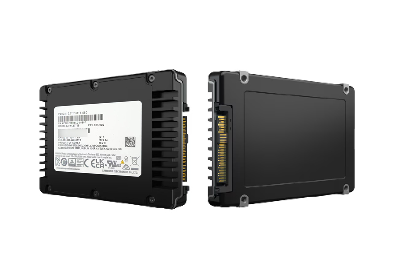 Samsung releases Gen5 SSD: Performance uation and application advantages of two PM1743 and PM9D3a models
 A Comprehensive Interpretation of RAID Cards: From Basic Knowledge to Brand Selection